

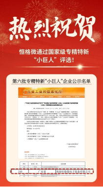
Recently, after review by the Ministry of Industry and Information Technology, various provinces and cities have successively announced the 6th batch of national-level "Little Giant" enterprises (specialized, sophisticated, distinctive, and innovative small and medium-sized enterprises). Hengge, with its continuous innovation and breakthroughs in the plasma field, has been honorably selected!
What is a "Little Giant" Enterprise?
"Specialized, Sophisticated, Distinctive, and Innovative" (SSDI) SMEs refer to small and medium-sized enterprises with the characteristics of "specialization, refinement, distinction, and innovation". Among them, SSDI "Little Giant" enterprises are located in the core areas of industrial foundation and key links of the industrial chain, with outstanding innovation capabilities, mastery of core technologies, high market share in niche segments, and good quality and efficiency, serving as the core force of high-quality SMEs. The SSDI "Little Giant" is the highest honor in China's SME sector, an important support for the future industrial chain, and a key force in strengthening, supplementing, and extending industrial chains.
At present, China has established a gradient cultivation system: Innovative SMEs → SSDI SMEs → National-level SSDI "Little Giants" → National Single Champion Enterprises in Manufacturing. In recent years, from the central to local governments, support for SSDI SMEs, especially "Little Giant" enterprises, has been further strengthened.
Whether an enterprise is selected as an SSDI "Little Giant" has become a standard for evaluating an enterprise's high-tech level and market position in the industry, as well as an important basis for enterprises to obtain financial support and subsidy policies such as equity and debt financing, mergers and acquisitions, and equity incentives. SSDI "Little Giant" enterprises are also key investment targets for local governments and have attracted much market attention.
Hengge focuses on industrial applications of plasma, devotes itself to R&D and innovation of plasma equipment, overcomes multiple technical difficulties, continuously breaks through technical bottlenecks, and has created a series of products with independent intellectual property rights and core technology patents.
Recently, our company has achieved two important technological achievements.
Achievement (1): PTH Inline Plasma Resist Stripping System
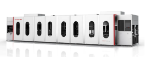
Industry First,an inline plasma resist stripping system that replaces wet process with dry process, eliminating the traditional PTH Desmear wet process flow.
It achieves 85% uniformity and a 60% increase in production efficiency; removes the Desmear section of PTH to reduce chemical usage and discharge; features eco-innovation by replacing wet process with dry process. Applied in PTH lines, it solves the problem of inline plasma treatment for large-area circuit boards.
Has passed CPCA Technological Achievement Review (Authentication)
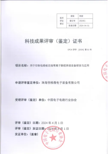
· Authentication Result ·
This system equipment is an industry first, with technical indicators reaching international advanced level. It has broad market prospects, and it is recommended to further promote its market application.
The equipment is currently undergoing DEMO testing at two leading enterprises.
It has completed trial production of over 40,000 pieces. Slice data shows that Plasma uniformity is better than PTH resist stripping effect. After Plasma treatment, the hole walls are smooth and uniform with good bonding strength.
Achievement (2): Deep Trench Etching Equipment
The "Deep Trench Etching Equipment" has been successfully developed. Test data shows that it has process indicators of high etching rate and high uniformity, reaching the level of internationally renowned brands.
It is suitable for 6-8 inch compound etching (SiC, GaN, SOI wafer), TGV, TCV and other processes. Different configurations can be selected to be compatible with TSV, DRIE and other processes.
A new starting point, a new development.
This honor will further inspire Hengge to continue adhering to the innovation-driven development strategy, give full play to the exemplary role of a national-level "SSDI Little Giant" enterprise, continuously enhance the core competitiveness of the enterprise, optimize product layout, expand domestic and international markets, and make greater contributions to promoting the high-quality development of the industry.